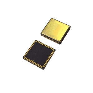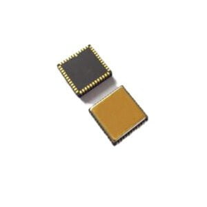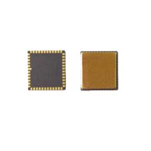
Regarding MEMS accelerometer the let us briefly introduce the package faetures about it.
MEMS technology is a fairly typical research and development field with multi-disciplinary cross penetration, strong comprehensive and cutting-edge fashion. It almost involves all the contents of natural and engineering disciplines, and takes monocrystal silicon Si, Si02, Sin, SOI and so on as the main materials. Si has excellent mechanical and electrical properties. Its strength, hardness and Yang modulus are similar to Fe, its density is similar to A1, and its thermal conductivity is similar to Mo and W. In the manufacturing of complex device structures, various mature surface micro-BD technology and body micro-machining technology are now being expanded to three-dimensional processing represented by LIGA (i.e., deep X-ray etching, micro electroforming, plastic mold) technology, micro powder casting, instant mask EFAB. Therefore, MEMS package has its own particularity significantly different from IC chip package:
(1) Specific
In MEMS, there are usually some movable parts or suspended structures, silicon cup cavities, beams, trenches, grooves, diaphragms, and even fluid and organic parts that basically work by surface effects. Packaging architecture depends on MEMS devices and uses. For MEMS devices with different structures and uses, the packaging design should be adapted to local conditions, synchronized with manufacturing technology, and has strong specificity.
(2) Complexity
Depending on the application, most MEMS packages need to have a non-electrical signal path directly connected to the outside world. For example, there is an input that transmits one or more information, such as light, magnetic, heat, force, chemical, etc. The complex interface of input signal puts forward special requirements for chip passivation and encapsulation protection. Some MEMS packaging and its technology is more novel than MEMS, not only the technical difficulty is difficult, but also the packaging environment cleanliness requirements up to 100 levels.
(3) Spatial
In order to provide enough moving and movable space for the MEMS movable part, it is necessary to etch or leave some grooves and other shapes of space on the shell. Packed MEMS needs clearance on the surface, which can provide a very effective protection cavity during packaging.
(4) Protection
MEMS made on a chip is extremely sensitive to the impact of the environment until it is packaged. Special treatment methods are required for each operation procedure, marking, sintering, interconnection and sealing of MEMS packaging, and corresponding protective measures are provided. A grid frame is installed to prevent mechanical damage to the movable parts. The circuit parts of the system must also be isolated from the environment to avoid affecting the performance of the processing circuit, and the packaging and its materials should not cause adverse effects on the environment in use.
(5) Reliability
MEMS is widely used, and higher reliability requirements are put forward for its packaging. In particular, it is required to ensure the safe work of products under harsh conditions and avoid harmful environmental erosion. Air tight packaging can dissipate excess heat.
(6) Economy
MEMS packaging mainly adopts customized research and development, which is still in the early stage of development, far from the requirements of serialization and standardization. Its packaging in the whole product price accounts for 40%-90% of the proportion, reducing packaging cost is a hot topic.
To sum up, the biggest difference between IC package and MEMS package is that MEMS generally needs to be contacted with the outside world, while IC is on the contrary. The main role of IC package is to protect the chip and complete electrical interconnection, and IC package cannot be directly transplanted into more complex MEMS. But in a broad sense, MEMS packaging form is mostly built on the basis of standardized IC chip packaging architecture. At present, most of the technologies follow the mature microelectronics packaging process, and to improve, evolution, to adapt to the special MEMS signal interface, shell, cavity, reliability, cost reduction and other requirements.
More Technical Questions
1.How to Distinguish MEMS Accelerometer and MEMS Gyroscope Correctly?
2.The Role of MEMS Accelerometers in Inertial Navigation
3.MEMS gyroscopes, accelerometers and magnetometers
4.How do MEMS gyroscopes work?
5.Application of MEMS Accelerometer in North Finder
6.MEMS Accelerometers and Piezoelectric Ceramic Accelerometers
Products in Article