With the development of MEMS technology, inertial sensor has become one of the most successful and widely used MEMS devices in the past few years, and mems accelerometer is an outstanding representative of inertial sensor devices. The theoretical basis of the mems accelerometer is Newton's second law, according to the basic principles of physics, within a system, the speed cannot be measured, but its acceleration can be measured. If the initial velocity is known, the linear velocity can be calculated by integrating, and the linear displacement can then be calculated. Combined with a gyroscope (used to measure angular velocity), the object can be precisely positioned. According to this principle, people have long used accelerometers and gyroscopes to navigate ships, planes and spacecraft, and in recent years, people have used this technology to autopilot cars and guided missiles. The rapid development of the automobile industry means that the accelerometer has found a new application field, and the anti-collision Air Bag of the car is controlled by the accelerometer.
The processes of capacitive MEMS accelerometers generally use: surface process, bulk silicon process, LIGA process and SOI + DRIE process, etc.
Surface technology is a micro-technology developed on the basis of integrated circuit planar technology, and only performs single-sided lithography. It uses the sequential deposition and selective etching of different materials on the silicon plane to form various microstructures. It mainly includes sacrificial layer deposition, sacrificial layer etching, structural layer deposition, structural layer etching, sacrificial layer removal (release structure), etc. Finally, the structural material is suspended above the substrate to form a two-dimensional or three-dimensional structure of various shapes.
The bulk silicon process refers to a process of etching a silicon substrate along the thickness direction of the silicon substrate, including wet etching and dry etching, and is an important method for realizing a three-dimensional structure. In order to form a complete microstructure, bonding or bonding technology is often used on the basis of processing, combining silicon bonding technology with bulk silicon processing methods. The microstructure of silicon is formed through multiple masking, single-sided or double-sided lithography and anisotropic etching, and then the relevant parts are precisely aligned and bonded into a whole. The bulk silicon processing technology process is more complicated than silicon surface processing, large in size and high in cost.
The SO1 + DRIE process is an extension and development of the bulk silicon process. The use of silicon-on-insulator (SOI) to fabricate single-crystal silicon three-dimensional microstructures has been an extremely rapid method in recent years. Almost all methods of manufacturing microstructures using SOI use DINE (deep reactive ion etching) to deeply etch single crystal silicon. Depending on the structure, performance requirements, etc., the front structure release and the back structure release can be used.
Development trend of MEMS accelerometers
(1) MEMS accelerometers with high resolution and large range have become the focus of research. Because the inertial mass block is relatively small, the inertial force used to measure acceleration and angular velocity is correspondingly small, and the sensitivity of the system is relatively low, so it is particularly important to develop a high-sensitivity accelerometer. Whether for civilian or military purposes, the mems accelerometer with high precision and large range will broaden its application range.
(2) Small temperature drift, small hysteresis effect has become a new performance goal, the selection of appropriate materials, the use of reasonable structure, and the application of new low-cost temperature compensation links, can greatly improve the accuracy of the micro-accelerometer.
(3) The development of multi-axis accelerometers has become a new direction. It has been reported that the triaxial micro-silicon accelerometer has been developed, but its performance is still far from practical, and the decoupling of multi-axis accelerometers is a difficult problem in structural design.
If you want to get more details about MEMS accelerometer,pls visit https://www.ericcointernational.com/gyroscope/mems-gyroscope/
More Technical Questions
1.Where Is The Quartz Accelerometer Used?
2.What is the use of quartz flexible accelerometer
3.What is the Purpose of the Accelerometer Senor?
4.Quartz Flexible Accelerometer for Inertial Navigation and Guidance Systems
5.Brief Introduction of Accelerometer
6.The Application of Accelerometer in Aircraft
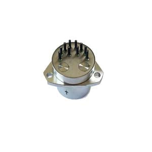
Products in Article