

The microstructure of MEMS gyroscope (microelectromechanical systems) needs to work in a vacuum environment to achieve a high resonance Q value and ensure its detection sensitivity. Vacuum packaging is also an important condition to ensure its detection accuracy. Wafer-level vacuum packaging is the mainstream process solution currently used for MEMS gyroscopes. Through wafer-level packaging, the microstructure of the MEMS gyroscope can be avoided from causing adhesion and particle pollution during the subsequent chip cutting process. It can also reduce the cost of vacuum packaging and improve the efficiency of MEMS gyroscopes. Chip processing yield. Wafer-level vacuum packaging can achieve device miniaturization and integration, and further improves the performance and reliability of MEMS gyroscopes to meet application needs in various fields.
This article aims to introduce the wafer-level vacuum packaging of MEMS gyroscope chips. The following will introduce the wafer-level packaging structure, process flow and key processes.
1. Wafer level packaging structure
Figure 1 shows the overall structure of the chip. The chip consists of a three-layer structure, namely the substrate layer, the device layer and the capping layer. The MEMS gyro microstructure in the device layer is the core part of the entire chip, and its periphery is a bonding ring, which is used to bond with the substrate layer and capping layer to form a sealed cavity structure. There is a layer of patterned silicon dioxide (SiO2) between the capping layer and the device layer. The device layer and capping layer are bonded together through silicon-silicon dioxide (Si-SiO2) direct bonding. SiO2 ensures that the device insulation layer and capping layer. There is an electrode pattern on the substrate layer, and the two layers are bonded together with the device layer through gold-silicon (Au-Si) eutectic bonding, forming a cavity that allows the comb microstructure of the device layer to move freely. And the side electrode lead-out method is used to realize the interconnection between the device layer structure in the cavity structure and the electrode pad outside the cavity.
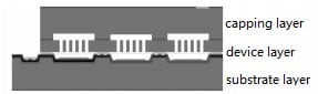
Figure 1 Wafer-level packaging MEMS gyroscope structure
2. Wafer level packaging process flow
Figure 2 will be divided into two parts, A and B. A shows the various processes of gyro chip capping and microstructure chip processing, and B shows the processing of the gyro substrate layer.
As shown in A, firstly, the anchor zone structure and cavity structure with SiO2 on the surface are formed on the capping layer by dry etching. The capping layer is then directly bonded to the device layer through Si-SiO2 direct bonding. Finally, after the device layer is thinned and polished, a dry etching process is used to etch the micro-movable structure of the gyroscope.
As shown in B, firstly, a cavity structure is formed on the substrate layer through wet etching, and an insulating layer is formed through thermal oxidation. Then an electrode layer is made on the insulating layer, and a second layer of SiO2 insulating layer is grown. Next, the second layer is formed. Contact holes are etched into the SiO2 insulating layer to facilitate the connection between the electrode and the subsequent gold layer. Finally, a getter film and an Au electrode are formed on the substrate layer, which are used for electrical interconnection and as a medium for subsequent Au-Si bonding.
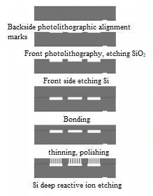
Figure 2(A) Device layer and capping layer process flow
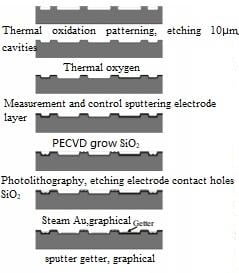
Figure 2(B) Substrate layer process flow
Wafer-level vacuum packaging of MEMS gyroscope chips is realized through Au-Si eutectic bonding. Under vacuum conditions, the Au on the substrate layer reacts with the silicon of the device layer to form a vacuum packaging of the chip. The heating process during the Au-Si eutectic bonding process can activate the getter, thereby improving the vacuum degree of the vacuum seal. Finally, after the chip is diced, the MEMS gyro chip shown in Figure 1 can be obtained.
3. Key processes of wafer-level vacuum packaging
3.1 Si-SiO2 direct bonding process
In the processing flow of the device layer and the capping layer shown in Figure 2(A), the direct Si-SiO2 bonding of the device layer and the capping layer is the core process to realize the microstructure of the device layer and the anchor area on the capping layer. mechanical connection.
The principle of Si-SiO2 direct bonding is that after cleaning, the bare Si wafer and the Si wafer with an oxide layer will form a hydrophilic surface with a high density of hydroxyl groups (-OH). The two wafers with hydrophilic surfaces will When bonded together, intermolecular forces (van der Waals forces and hydrogen bonds) will bond the two wafers together. After the wafer is annealed, the active hydroxyl groups combined with each other begin to dehydrate and will be converted into stable Si-O-Si covalent bonds, forming a permanent Si-SiO2 bonding interface.
In the above process, the hydroxyl groups on the surface of the wafer are an important medium for the bonding of the wafer. Therefore, during the cleaning process of the Si wafer, the Si wafer that has been cleaned by standard no longer uses hydrofluoric (HF) acid to remove the natural oxide layer to ensure that the wafer The hydrophilic state of the surface. In order to improve the bonding strength, oxygen plasma and nitrogen plasma activation treatments were performed on the surfaces of the bare Si wafer to be bonded and the Si wafer with oxide layer, respectively. After plasma activation treatment, the dangling bonds of active hydroxyl groups on the surface of the wafer to be bonded will be increased, which is beneficial to improving the bonding strength. In order to ensure that the gyroscope works stably and reliably, all anchor points on the gyroscope microstructure need to have high bonding strength.
3.2 Research on getter technology
In wafer-level packaging MEMS gyroscopes, getter film preparation is a necessary method to obtain high vacuum and ensure high Q value of gyroscope resonance. The getter material needs to be heated and activated under vacuum conditions to restore its getter ability. The activation of the getter usually needs to be carried out at the same time as the final vacuum packaging process of the chip. Therefore, in the process flow designed in this article, the activation of the getter needs to be compatible with the Au-Si eutectic bonding process. The activation of the getter The temperature should be lower than the eutectic temperature of Au-Si alloy (363°C).
3.3 Au-Si eutectic bonding vacuum packaging process
Wafer-level vacuum packaging of MEMS gyroscopes is achieved through Au-Si eutectic bonding. Au-Si bonding is a key link in wafer-level vacuum packaging. While achieving wafer-level vacuum packaging of MEMS structures, MEMS The electrical connection between structure and circuit leads. Align the processed substrate sheet, device layer and capping layer as shown in Figure 2(A) and Figure 2(B) under the bonding aligner, and then put them into the bonding machine for Au-Si bonding . After high-temperature degassing during the bonding process, the two sets of wafers were brought into contact and a pressure of 5000N was applied. After the temperature rose to the eutectic point of 363°C, it was held for 15 minutes, and then continued to rise to 400°C and held for 15 minutes to ensure that the Au -Si eutectic reaction is sufficient.
Au-Si eutectic bonding is very sensitive to the oxide layer existing on the Si surface. The wettability of Au on the SiO2 surface is very poor, and the natural oxide layer of the Si sheet will prevent Au-Si contact, making eutectic fusion impossible. Therefore, in order to ensure that the Au-Si bond has sufficient bonding strength, the natural oxide layer on the Si surface needs to be removed with dilute hydrofluoric acid before bonding. However, during the wet cleaning process with dilute hydrofluoric acid, the surface tension of water molecules can easily cause adhesion of the comb teeth or beam structure. In order to avoid adhesion of the microstructure, a gaseous hydrofluoric acid dry etching process is used to etch away the natural oxide layer on the surface. Since the comb tooth structure of this process does not need to be immersed in liquid, it will not cause structural adhesion.
During the Au-Si eutectic bonding process, the liquid phase eutectic alloy generated by Au-Si is prone to overflow under pressure. Au-Si eutectic overflow can easily cause short circuits between microstructures and affect chip yield. In order to ensure good bonding quality and prevent the overflow of the eutectic liquid, an anti-overflow shallow groove structure can be designed on the sealed bonding ring around the gyroscope. During the bonding process, the liquid Au-Si eutectic is first filled into the shallow grooves under the action of pressure, thus avoiding the overflow of the Au-Si eutectic liquid and the short circuit of the structure.
4.Conclusion
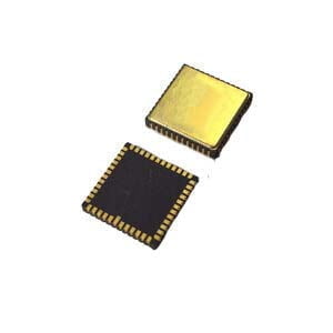
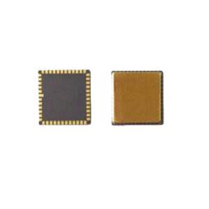
This article studies the wafer-level vacuum packaging of MEMS gyroscope chips, and explains the wafer-level packaging structure, process flow and key processes. Since the accuracy of the MEMS gyroscope is a decisive factor in its performance, and wafer-level vacuum packaging is an important condition for testing its accuracy, the wafer-level vacuum packaging of the MEMS gyroscope is important knowledge to understand. The ER-MG2-50/100 developed and produced by Ericco uses a hermetically sealed ceramic LCC surface mount package and is capable of operating with a 5V power supply and a wide temperature range (−40°C to +85°C).
If you want to learn more about MEMS gyroscopes, please click on the relevant articles and related products below to continue learning.
More Technical Questions
1.Noise Analysis and Solutions of MEMS Gyroscope
2.What’s the north-seeking principle of MEMS gyroscope?
3.The materials and structure of MEMS gyroscope
4.MEMS gyroscope VS FOG: What’s the difference between them?
2.How does MEMS gyroscope work in harsh high temperature environment?
6.Gyroscope technology development: Why MEMS gyroscope stands out?
Products in Article
.jpg)